This is a
version of:
Technical Report No. 301L
Submitted to the School of Electrical and Computer Engineering
Chalmers University of Technology
in partial fulfilment of the requirements for the degree of
Licentiate of Engineering


Microwave Electronics Laboratory
Department of Microelectronics
Chalmers University of Technology
S-412 96 Göteborg, Sweden
November 1998
ISBN 91-7197-743-0
Phase noise is the limiting factor in almost all microwave systems as of today. The phase noise causes decreased resolution in radar systems, symbol interference in transmission links, restricted resolution in spectrum analysers and more. Of course, the industry of today is interested in finding solutions to these problems.
The aim of this work is to report about different published techniques, extended with my own work and ideas, on how to design low phase noise electronically controlled oscillators for micro- and millimetre wave frequencies.
First the report goes through the most important definitions on phase noise. After that, the sources of noise, the oscillator operation and the phase noise generating process is examined. Finally, an extensive and occasional profound list of different methods for designing low phase noise oscillators is compiled.
Techniques for measuring phase noise are not covered. Outer arbitrary effects such as mechanical vibrations, load variations, noise from bias sources and temperature drift are not covered as well. Neither is techniques employing cryogenic temperatures covered. The problem of simulating the phase noise in oscillators is only briefly discussed.
Keywords: phase noise, FM noise, PM noise, noise, microwave, millimetre wave, mm-wave, radio, RF, oscillator, VCO, 1/f noise, oscillation criteria, resonator, delay line, stabilised, quartz crystal, phase error, microstrip resonator, cavity resonator, dielectric resonator, DR, DRO, surface acoustic wave, SAW, sapphire resonator, whispering gallery mode, YIG sphere, YIG film, fibre optic, Fabry-Perot resonator, device, silicon bipolar transistor, Si BJT, gunn diode, MESFET, HEMT, HFET, PHEMT, HBT, amplitude limiter, automatic gain control, AGC, clipping diode, varactor, anti series, piezo electric, magnetostrictive, terfenol, multiplier, phase locked loop, PLL, frequency discriminator, balanced oscillator, transposed gain, laser.
Consider an oscillator output signal g(t) with a phase distortion Φ(t)
| g(t)=Acos[2πf0t+Φ(t)] | (1) |
Compiled from [1], [2], [3] and [4] we have the spectral density of phase fluctuations SΦ (units rad²/Hz)
| (2) |
where the capital F denotes the Fourier transform and fr denotes the frequency deviation with respect to the carrier frequency f0. (fr=f−f0)
The spectral density of frequency fluctuations is (units Hz²/Hz)
| (3) |
The most commonly used quantity to characterise phase noise is the single sideband noise to carrier ratio in dBc/Hz
| (4) |
where PC is the power in the carrier and PSSB is the single sideband power created by the phase distortion. A small angle approximation can be made if Φ(t)<<1, with the result that SΦ(fr) can be interpreted as the double sideband noise to carrier ratio. In this case, the single sideband noise to carrier ratio in dBc/Hz is
| (5) |
The small angle approximation is valid for L(fr) values up to approximately −20 dBc/Hz, which is sufficient in almost all practical cases concerning low phase noise oscillators. Complicated modulation theory incorporating Bessel functions is necessary above this level.
For example, suppose that the phase distortion is
| (6) |
and
| Φ0RMS<<1 | (7) |
In this case the spectral density of phase fluctuations (2) becomes
| (8) |
Going back to the oscillator output signal (1) and inserting the phase distortion (6) one gets
| (9) |
which has the power density spectrum (units V²/Hz, A²/Hz...):
| (10) | ||||||||||||||||
where, f denotes the absolute frequency (f = f0+fr).
| The term | A² | δ(f−f0) represents the carrier, and the term |
|
{δ[f−(f0−fm)]+δ[f−(f0+fm)]} represents two sidebands. | |||
| 2 | 4 |
| (11) | ||||||||||||||||
The single sideband noise to carrier ratio in dBc/Hz becomes:
| (12) |
The same result would appear using (5) and (8).
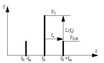
Figure 1 Power density spectrum of exemplified oscillator signal.
One way of looking at oscillator phase noise is to study how the oscillator transforms basic noise sources into phase noise. To do this, it is necessary to study the functionality of the oscillator, and have some knowledge of noise sources.
Different forms of noise sources are [5]:
Shot noise originates from the random passage of carriers across a junction in a transistor or a diode, with the spectral density
| (13) |
where q is the electron charge, I is the average current and Δf is a bandwidth.
Thermal noise originates from the random thermal motion of electrons in a resistor R, with the spectral density
| (14) |
where k is Boltzmann's constant, T is the absolute temperature and Δf is a bandwidth.
This type of noise is also frequently referred to as 1/f-noise. The origin of flicker noise is still a matter of discussion. Flicker noise is present in all active, and some passive devices and always in association with a direct current flow. The spectral density is
| (15) |
where
K is a constant for a particular device,
I is the average current,
a is a constant in the range 0,5 to 2,
f is the frequency,
b is a constant about unity and
Δf is a small bandwidth at frequency f.
Burst noise is also referred to as popcorn noise and g-r (generation recombination) noise. The origin is a matter of discussion as well. The spectral density is
| (16) |
where
K is a constant for a particular device,
I is the average current,
a is a constant in the range 0,5 to 2,
f is the frequency,
fgr is a particular frequency for a particular noise process and
Δf is a small bandwidth at frequency f.
Burst noise often occur with multiple time constants, and this gives rise to multiple humps in the low frequency parts of the noise spectrum. At higher frequencies the white noise of thermal and shot noise dominates. The frequency at which the white noise level is equal to the flicker noise level is referred to as the corner frequency fc. The spectral density of composite noise can appear as in figure 2.
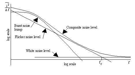
Figure 2 Spectral density of composite noise.
In this section, first the simple criteria for oscillation in a noiseless oscillators will be treated and then a discussion on the phase noise generating process in oscillators is carried out.
First, consider the two interconnected multiport networks with scattering parameter matrices S1 and S2 in figure 3.
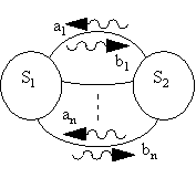
Figure 3 Two interconnected multiport networks.
We have the wave vector
| (17) |
and also the wave vector
| (18) |
Combining (17) and (18) one get
| (19) |
which can be rearranged into
| (20) |
where I is the unit matrix. The non-zero solution representing a possible oscillation is
| det(I−S1S2)=0 | (21) |
This deduction can also be found in [6]. A stability criteria, which will be treated in section 4.2 "Operation point stability", must be met together with this necessary oscillation criteria for a stable oscillation.
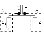
Figure 4 Reflection-, or negative resistance oscillator.
In this case the two networks S1 and S2 consists of two impedances Z=R+jX and Za=Ra+jXa. One of the two impedances have a negative real part (Ra<0). The related reflection coefficients Γ and Γa, are described by
| (22) |
and
| (23) |
The oscillation criteria (21) becomes
| det(1−ΓaΓ)=0 | (24) |
with the solution
| (25) |
where n is an integer. In section 3.2.2 and section 4.1.1 it will be shown that a larger value of n can lower the phase noise. Unfortunately, it also dramatically increases the risk of unwanted spurious oscillations.
Here one should keep in mind that the active device giving the reflection coefficient greater than 1 has a bigger small signal value than large signal value due to the saturation at steady state oscillation. A margin in the order of a few decibels is therefore needed as a start-up criteria, since the greater-than-1-reflection-coefficient given by the active device will decrease as the oscillation builds up to the steady state level, which is given by the saturating level of the active device.
| (26) |
With impedances we get from (22), (23), (25)
| (27) |
which can be rearranged into
| (28) |
with the solution
| Za+Z=0 ⇒ Ra=−R & Xa=−X | (29) |
Here too, one need a margin factor for the ratio of the small signal negative resistance −Ra over the load resistance R of the order of a few times for oscillation to start. Often a −Ra/R ratio of 3 is sufficient.
| Ra>−R & Xa=−X | (30) |
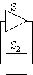
Figure 5 Transmission mode oscillator.
In this case the two networks S1 and S2 consists of an amplifier and a feedback network, with scattering parameter matrixes
| (31) |
and
| (32) |
the oscillating criteria (21) becomes
| (33) |
which simplifies into
| (34) |
and further into
| (35) |
with the solution
| (36) |
Here too, one need a margin for the amplification in the order of a few decibels, usually the level 3 dB is mentioned, and the integer n should be chosen carefully.
| (37) |
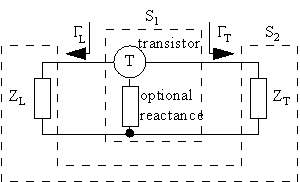
Figure 6 Transistor oscillator.
A transistor with one connector grounded, possibly via some reactance, as depicted in figure 6, form a two-port network described by the scattering parameter matrix
| (38) |
It could for example be a field-effect transistor with its source grounded or a bipolar transistor with its base grounded via an inductor. Two impedances ZL and ZT with reflection coefficients ΓL and ΓT, as depicted in figure 6 form a two-port network described by the scattering parameter matrix
| (39) |
The two impedances ZL and ZT could for example be a resonator and a load. Interconnecting the two two-port networks S1 and S2, as depicted in figure 6, one gets a possible oscillator. The oscillating criteria (21) becomes
| (40) |
which simplifies into
| (41) |
with two different possible formulations
| (42) |
with the well known solutions
| (43) |
The oscillation criteria will be fulfilled if either one of the two criterias are met since they both derive from the same oscillation criteria equation.
Consider a simple oscillator consisting of an amplifier and a feedback path as illustrated in figure 7.
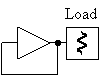
Figure 7 Simple oscillator.
Oscillation starts by amplification of noise. If the amplifier was all linear, the amplitude in this oscillator would either decrease to zero or grow to infinity depending on the total gain in the loop (> 0 dB). Lets assume that the small signal loop gain is greater than 0 dB. Real amplifiers always have some amplitude non-linearity, usually provided by gain compression. That is, the gain compression decreases the loop gain above a certain amplitude level, thereby stabilising the amplitude level to a fixed value. Let us extract this amplitude non-linearity (with zero phase shift) from our amplifier to a separate block and consider our amplifier being somewhat more linear, see figure 8.
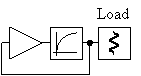
Figure 8 Simple oscillator model with semi linear amplifier.
The frequency of oscillation is given by equation (36), that is (S21 refer to the amplifier)
| ∠S21|f = n·360° | (44) |
This frequency of oscillation may not be equal to a desired frequency of oscillation. Therefore, an additional phase shift for example in the form of a transmission line with delay time τ can be inserted to shift the frequency to a desired value, see figure 9.
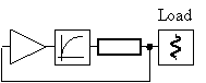
Figure 9 Oscillator model with semi linear amplifier.
Now the frequency of oscillation is given by the condition
| ∠S21|f +2πfτ = n·360° | (45) |
The solution is illustrated in figure 10.
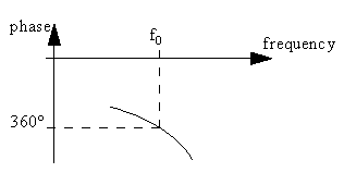
Figure 10 Frequency of oscillation.
There are voltage dependent reactances present in the amplifier (for example a reverse biased pn-junction) which are effected by noise (see section 3.1, "Sources of noise"). These noise effected reactances cause the phase shift of the amplifier to vary. Therefore we extract a noise driven phase shifter from the amplifier in our oscillator model and consider the amplifier to be completely linear after that. See figure 11.
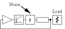
Figure 11 Oscillator model with linear amplifier.
The model is also useful for reflection type oscillators if modified into the circuit depicted in figure 12.
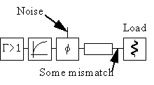
Figure 12 Reflection oscillator model with linear device.
The oscillator models reveals three different phase noise generating processes:
Of the above phase noise generating processes, the first two that are caused by low frequency noise usually dominate. Most, if not all, methods for designing low phase noise oscillators approaches the problem accounting for one or more of the three above processes.
A small phase shift ΔΦ in the noise driven phase shifter causes a small shift in frequency of oscillation Δf as depicted in figure 13:
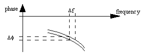
Figure 13 Phase to frequency dependency.
We have
| (46) |
The spectral density of frequency fluctuations using equation (3) becomes
| (47) |
where S'Φ(fr) denotes the spectral density of phase fluctuations for the open loop amplifier, not the closed loop oscillator. Using (3) again, the closed loop oscillator spectral density of phase fluctuations becomes:
| (48) |
This equation is valid close to the carrier only. The closed loop spectral density of phase fluctuations is expected to be equal to the open loop spectral density of phase fluctuations for large fr values. We extend the equation to cover these values as well:
| (49) |
A similar deduction can be found in [1]. The usefulness of this equation is that it gives an explanation to the observed spectral densities of oscillations. However, it's very difficult to calculate the open loop spectral density of phase fluctuations S'Φ(fr) since closing the loop alters the conditions for the noise levels due to non-linear effects. Nevertheless, the open loop spectral density of phase fluctuations S'Φ(fr) is expected to be on the form as depicted in figure 2. Neglecting burst noise one get
| (50) |
The resulting closed loop spectral density of phase fluctuation, including some burst noise, for the two cases
| (51) |
and
| (52) |
are depicted in figure 14
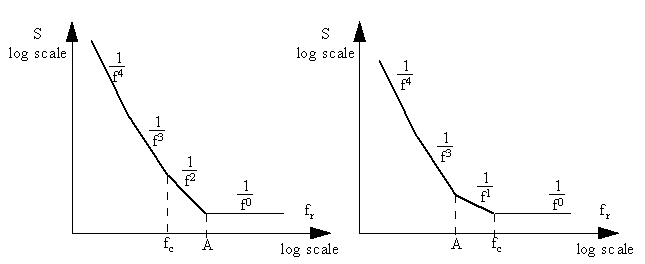
Figure 14 Oscillator phase noise spectral densities.
The different sections are:
1/f4 Modulated burst noise
1/f³ Modulated flicker noise
1/f² Modulated white noise or unmodulated burst noise plateau
1/f1 Unmodulated flicker noise
1/f0 Unmodulated white noise
Equation (48) indicates a possibility to reduce the phase noise by inserting a steep phase to frequency derivative block in the oscillator. Resonators and delay lines can provide such steep phase to frequency derivative. They will be treated in this section.
Consider the series resonant circuit in figure 15.
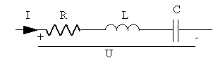
Figure 15 Series resonator.
The current is
| (53) |
At resonance we have
| (54) |
and the definition
| (55) |
The L-index on QL is for to clarify that this is the operating, or loaded-Q. Inserting (54) and (55) into (53) we get
| (56) |
Similarly, consider the parallel resonant circuit in figure 16.
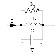
Figure 16 Parallel resonator.
The voltage is
| (57) |
similarly, at resonance we have
| (58) |
and similarly, the definition
| (59) |
inserting (58) and (59) into (57) we get
| (60) |
The similarities between (56) and (60) are obvious. In both series (figure 15) and parallel (figure 16) resonators the current or voltage to maximum current or voltage ratio is
| (61) | ||||||||||||||||||||||||||||
With the phase being
| (62) |
and the phase to frequency derivative
| (63) | ||||||||||||||||||||||||||||||||||||||||||||||||||||||||||||||||||||||||||||||||||||
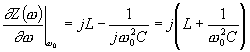
at resonance we get
| (64) |
Inserting (64) into (48) results in
| (65) |
which is sometimes referred to as the Leeson model [1]. As seen in (65), maximising the loaded quality factor QL minimises the phase noise. It is a generally accepted method [2], [7], [8], [9]. It should be pointed out that if the resonator's own flicker noise dominates in the phase noise generating process there will be no reduction of the phase noise due to an increased loaded quality factor QL [2], [10]. The situation is rare, and only appears when the resonator incorporates some biased device, for example a biased laser diode in a fibre optic delay line resonator.
The resonator, labelled "Q" may be connected inside the oscillating loop:
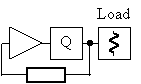
Figure 17 Feedback oscillator with resonator.
It is very important to design the phase shift in the oscillation loop correctly so that the frequency of oscillation is equal to the resonators resonant frequency, where its phase to frequency derivative is maximum [11]. A phase error Φ in the feedback loop has been shown to strongly degrade the phase noise performance of the oscillator with a 1/cos4Φ dependence [12].
In another method of connecting a resonator one uses a circulator as in figure 18. This is sometimes referred to as "self injection locking" [13], [14].
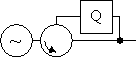
Figure 18 Self injection locked oscillator.
Long delay lines are also capable of providing a steep phase to frequency derivatives. Such delay lines should not be confused with transmission lines used as resonators where their ends are loosely coupled. With long delay lines one need to take extra care to avoid spurious oscillations. The phase of a delay line is
| Φ = −2πfτ | (66) |
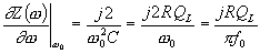
where τ is the delay time. Using (64) one gets a corresponding quality factor for delay lines
| (67) |
The choice of resonator is often affected by other aspects than the quality factor, such as available space, cost etceteras. Generally, reflection mode resonators can have a larger loaded quality factors than transmission mode resonators since they have fewer ports causing power loss, and thereby are less loaded.
The simplest form of resonators are lumped inductor capacitor resonators. Their quality factors are poor since the inductors usually have a considerable resistance.
Quartz crystals are inexpensive and have excellent quality factors. They are the standard solution in the KHz and MHz range.
Loosely coupled sections of open- or short circuited transmission lines are used in the 100 MHz to 1 GHz range, see figure 19. Typical values for quality factors range from several hundreds up to about 10 000 [15].
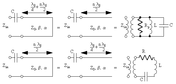
Figure 19 Transmission line resonators.
Microstrip resonators typically produce quality factors in the range 100 to several hundred [15]. Some examples of microstrip resonators are depicted in figure 20.
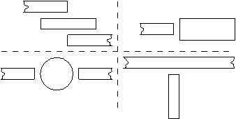
Figure 20 Microstrip resonator examples.
Cavity resonators can produce quality factors in the range 10 000 to 40 000 or more [15]. For example, the optimum quality factor of a TE011 mode cylindrical copper cavity (see figure 21) is approximately [15]
| (68) |
which equals 42 426 for a 5 GHz cavity.
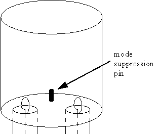
Figure 21 Cavity resonator.
Dielectric resonators (see example in figure 22) have typical quality factors ranging from around 100 to several hundred. Normally the dielectric resonator is enclosed in a shielding box, and then the quality factor can approach the intrinsic quality factor of the dielectric material, which is equal to the reciprocal of the loss tangent. (in the range 2 000 to 28 000). Dielectric resonators are often preferred before cavity resonators due to their compactness, originating from the dielectric resonator's high dielectric constant [15].
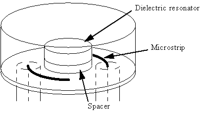
Figure 22 Dielectric resonator.
Surface acoustic wave (= SAW) delay lines sometimes find their use as providers of steep phase to frequency derivatives.
Sapphire resonators in the whispering gallery mode can produce such high quality factors as 185 000 [16].
Yttrium-iron-garnet (YIG) is a frequently used material for resonators since its resonant frequency can be directly tuned by a biasing magnetic field. YIG-spheres are capable of quality factors of the order of ~200 [17]. Magnetostatic surface wave oscillators [18] made out of YIG-film can produce quality factors of ~1 800 [17]. Although their quality factors are not as high as other types of resonators, they will not be degenerated by the loading of a varactor since they can be tuned directly. Indeed a highly desirable property, enabling low phase noise and broad tuning range oscillators.
A fibre optic transmission line used as a delay line can produce a very high quality factor since it can easily be made very long without troublesome losses. A 6,2 km long fibre optic transmission line used at 7,2 GHz in [10] and [19] implies a quality factor of approximately 500 000 to 1 000 000.
Fabry-Perot resonators (see figure 23) are used from millimetre wave frequencies and beyond. They consists of two mirrors, or a cavity without side walls, capable of producing quality factors as high as 5 000 000 for submillimetre waves. The quality factor of a parallel (spacing d) copper plate Fabry-Perot resonator is approximately [20]
| (69) |
which for a 4 cm spaced 94 GHz resonator equals 92 000.
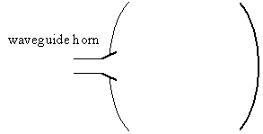
Figure 23 Fabry-Perot resonator consisting of two mirrors and a waveguide horn.
If feedback modified white noise dominates in the phase noise (which is usually not the case [2], [9], [21]), then the ratio of loaded quality factor to unloaded quality factor QL/Q0 can be optimised for minimum phase noise. That is a situation when SΦ(fr) is proportional to 1/fr² and it isn't a feedback modified burst noise plateau. First, consider the resonator in figure 24
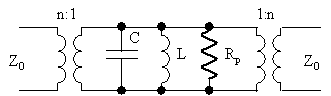
Figure 24 Resonator.
The unloaded quality factor Q0 is as before (59)
| (70) |
while the loaded quality factor QL is (59)
| (71) |
combining (70) and (71) we get
| (72) |
The net reactance is null at resonance. Therefore, at resonance the resonator consists of three building blocks described by two transformers and one resistor. The transformers (figure 25)
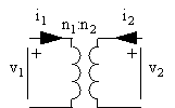
Figure 25 Transformer.
are described by the ABCD-matrix equation
| (73) |
and a resistor (figure 26)
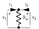
Figure 26 Resistor.
is described by the ABCD-matrix equation
| (74) |
The complete resonator, at resonance, is described by the ABCD-matrix
| (75) |
from which we can calculate [22]
| (76) |
Using (72) one finds
| (77) | ||||||||||||||||||||||||||
Now, looking back at figure 17 one realises that the amplifier gain G will have to overcome the resonator loss (77) and some other losses Lo in the feedback loop, that is
| (78) |
With the amplifier being noisy with noise figure F and using (78) we get the spectral density of the output noise from the amplifier [5]
| (79) |
where Ni is some white noise level at the input port, for example thermal noise. This noise will then generate open loop phase fluctuations due to AM-FM conversion with some proportionality constant, in this case called "B". When the oscillator loop closes, these phase fluctuations gets modified according to (65) resulting in a closed loop spectral density of phase fluctuations
| (80) |
For to find its minimum value we first calculate it's derivative
| (81) |
and setting the derivative equal to zero one gets
| (82) |
Similar deductions giving the same result can be found in [2] and [23]. In [24], [25] and [26] it is suggested that the value for QL/Q0 could be the above as suggested, or equal to 2/3. One should also keep in mind that the noise figure is dependent of the impedance at the amplifier's input port, see section 4.5.
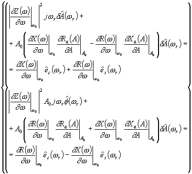
Following the outline in [27] we consider the simplified oscillator circuit in figure 27 below, where the non-linear amplitude dependence is put into an active device Za(A(t)), and the linear frequency dependence to a passive component Z(ω).
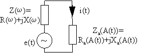
Figure 27 Simple oscillator circuit.
Using (29) on the oscillating circuit we get
| Z(ω0)+Za(A0)=R(ω0)+jX(ω0)+Ra(A0)+jXa(A0)=0 | (83) |
The disturbed oscillating current i(t) is
| i(t)=A(t)cos[ω0t+Φ(t)] | (84) |
where the amplitude A(t) and phase Φ(t) only varies slowly compared to ω 0. The time derivative of the current becomes
| (85) |
In the steady state case, a time derivative equals multiplication by jω. Thus, in this semi-stationary case the disturbed oscillation can be described with a complex angular frequency
| (86) |
Since the phase Φ(t) and amplitude A(t) only varies slowly we can expand the impedance Z(ω) in a Taylor series around the angular frequency ω0.
| (87) |
Similarly we can expand the impedance Za(A(t)) in a Taylor series around the mean amplitude level A0.
| (88) |
the distortion voltage in figure 27 is
| e(t) = [Z(ω)+Za(A(t))]i(t) = Re{[Z(ω)+Za(A(t))]A(t)ej[ω0t + Φ(t)]} | (89) |
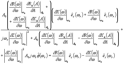
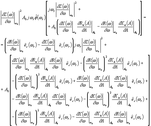
Following the deductions in Appendix A this leads to
| (90) |
Which is the criteria for a stable oscillation. Of course, if it does not apply there will be no oscillation. It has a graphical interpretation which can be found by letting
| (91) |
and
| (92) |
Then (90) becomes
| (93) |
which can be simplified into
| (94) |
and further into
| sin(β−α)>0 | (95) |
which gives
| 0<β−α<π | (96) |
The graphical interpretation is depicted in figure 28 where the arrows indicate increasing angular frequency and amplitude respectively.
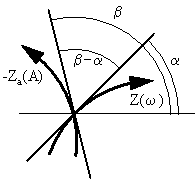
Figure 28 Graphical interpretation of stability criteria.
The graphical interpretation also holds for scattering parameters since the Smith chart is simply a conform reproduction which preserves the angles. In this case the curves should be
| (97) |
and
| (98) |
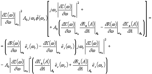
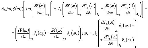
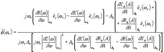
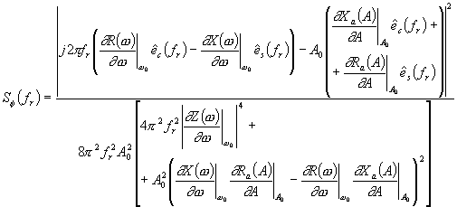
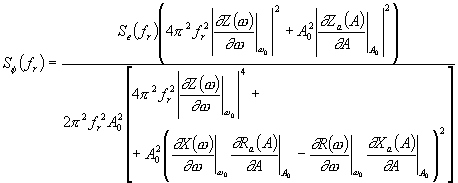
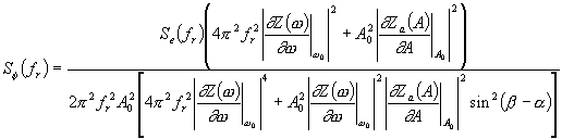
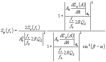
In Appendix B it is shown that the spectral density of phase fluctuations for the oscillator in figure 27 is
| (99) |
The optimum value is obtained for β−α=90°. Common sense tells that this is minimising the AM to PM conversion coefficient.
| (100) |
The method is recognised by [7], [8], [21] and [9] among others. It is a striking resemblance between equation (100) and (65). Even more if one consider that the distortion voltage is amplitude dependent.
Increasing the oscillator power level does not result in a direct reduction in oscillator phase noise level [2] even though equation (100) implies that increasing the power level P
| (101) |
should lower the phase noise. One reason for this can be that an increased power level usually requires an increased bias current, and the fact that the noise sources that has the greatest effect on the phase noise are current dependent (15), (16).
All phase fluctuations will add linearly in an oscillator loop. There is no first critical block as in a reciver where the first low noise amplifier dominates. Thus, a multistage amplifier will generally have a higher flicker noise level than a single stage amplifier [2].
Of course, one should choose a device with small low-frequency noise [7], [8]. The options are limited by a number of factors such as if the device is available at an acceptable price for the design frequency and if the device is compatible with intended manufacturing process etceteras.
It is difficult to draw any conclusions from comparisons between different oscillator circuits since it is difficult to know exactly what one is comparing. Questions that arises are: is the devices operating on its optimum bias point, what low frequency impedance is the device exhibiting and what quality factor had the resonator? Nevertheless, the combined experiences from a number of authors give some aid in the decision making.
The silicon bipolar transistor (Si BJT) is probably the best choice when it comes to phase noise [8], [28], [29] and [9]. [9] mentions gunn as the second best choice. Good results have been reported with heterojunction bipolar transistors (HBT), and especially with indium phosphide (InP) based ones [30], [31]. Pseudomorphic high electron mobility transistors (PHEMT's) have been found to be better than HBT's [32]. PHEMT's have been found to be equally good with metal semiconductor field effect transistors (MESFET), that are usually better than high electron mobility transistors (HEMT) [33], [34].
The above and phase noise levels mentioned in the references can be summed up in the following ranking list:
The ongoing improvements in device technology, inconsistent terminology (PHEMT's being called HEMT's etceteras.) complicates the picture. One can see that the low-frequency noise level are usually higher in field effect transistors (probably due to the lateral structure) than in bipolar transistors (probably due to the vertical structure), but on the other hand, the up-conversion mechanism is worse in bipolar transistors (probably due to a more non-linear function). Aluminium doping have been found to increase the low-frequency noise level. Field effect transistors are a few years more mature than bipolar transistors at high frequencies.
If white noise dominates in the phase noise generating process, which is usually not the case [2], [9], [21], then the source impedance for the amplifying part in a oscillator should be optimised at the oscillation frequency [8] just as in the case of an low noise amplifier. That is, in a situation when the spectral density of phase fluctuations SΦ(fr) is white or proportional to 1/fr² and it isn't a modulated burst noise plateau.
Also, keep in mind that altering the source impedance can (will) alter the unloaded to loaded quality factor ratio QL/Q0, as in section 4.1.2 "Optimal coupling".
Improvements in the order of 15 dB have been reported by simply aiming at a oscillator circuit design with minimum frequency sensitivity to a small bias change (minimum "pushing" sensitivity) [7], [21], [35], [36].
It has been stated that a phase noise minimum can be found for a specific bias collector current level in HBT oscillators [32], [37]. [32] finds the same to be true for HEMT's. In [38] a minima is also found for a specific drain voltage applied to a GaAs MESFET. An improvement of the order of 15 dB is observed. In [29] it is found that the phase noise is less at a high bias collector current level.
Since feedback modified low frequency noise usually dominates the phase noise in an oscillator one should aim to find the optimum source and load impedance for the amplifying part at low frequencies in analogy with an normal low noise amplifier [39], [40], [29], [41], [42]. The effect applies for both field effect transistors and bipolar transistors. The source impedance for an field effect transistor is found to be optimum when high (hundreds of kΩ's). Improvements in phase noise level of approximately 10 dB have been observed.
An appropriate low frequency feedback between the transistors drain/collector and gate/base can reduce the phase noise [39], [40] even though feedback has no effect on the noise performance in the linear case [5]. The results are modest, probably due to a sometimes low correlation between the phase noise and the low frequency current noise at the transistor drain side [43], [44], [45].
Phase noise is partly generated trough a mixing process in the amplitude limiting non-linearity between the oscillation frequency and the low frequency noise, see section 3.2.2. The amplitude limiting non-linearity and the amplifying parts are usually integrated into a single transistor which operates compressed, and the dominating low frequency noise source is usually situated in that compressed transistor. Therefore, the low frequency noise has direct access to the amplitude non-linearity, and of course then mixes with the oscillation frequency. An idea for to reduce this effect is to separate the amplifying part from the amplitude limiting part by using some automatic gain control (= AGC) or clipping diodes (see figure 29) [8], [40], [46]. Improvements in the order of 15 dB have been observed.
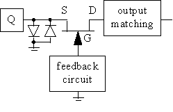
Figure 29 Oscillator with amplitude limiting clipping diodes.
When tested [46], clipping diodes were used. It seams that the clipping diodes were then directly connected to the amplifying transistor. It would probably be advantageous to have a low frequency blocking in between, for to prevent the low frequency noise from the transistor to reach the non-linearity in the clipping diodes where it can mix with the oscillation frequency and create phase noise. No references on such an improved idea have been found.
The simplest technique for to electronically control an oscillator is by controlling some bias voltage that influences for example a pn-junction capacitance. This is sometimes referred to as "bias pushing". The technique exhibits low cost feature since no extra tuning device is needed, but suffers from poor phase noise performance, see section 4.5. The tuning range is expected to be small since it is difficult to fulfil the oscillation criterias when the bias point is changed.
A somewhat improved solution when it comes to phase noise is to use a separate varactor diode for frequency tuning. The quality factor of a varactor diode is poor compared to most used resonators, and will degrade the resonator accordingly. The material in the diode, doping profile etceteras influences the usefulness of the diode. A small low-frequency noise level is of high concern.
The use of a "linear varactor", see figure 30, is reported to give a 10–15 dB improvement over the use of conventional varactors [47].
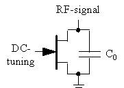
Figure 30 Linear varactor.
The use of two anti series coupled varactors, see figure 31, is reported to give a 5–10 dB improvement over the use of conventional varactors [48] due to an more linear capacitance, and thereby less mixing of low frequency noise with the oscillation frequency. A better temperature stability is also observed.
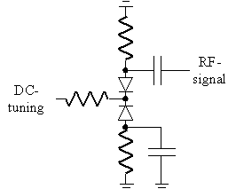
Figure 31 Anti-series connected varactors.
YIG equipped oscillators are used where high performance is of greater concern than cost, for example in measurement instruments, see section 4.1.1 "Resonators".
Narrow-band piezo electric tuning of a cavity is mentioned in [9], [49] and [50]. The technique is reported not to degrade the quality factor of the resonator, which of course gives excellent phase noise performance. The tuning range is poor, unless some mechanical gearing for improved displacement is used.
No references on the use of magnetostrictive materials such as terfenol instead of piezo electric materials for narrow band mechanical tuning of a cavity have been found. Magnetostrictive materials have a much greater expansion coefficient than piezo-electric materials, but are more expensive.
There are some publications on magnetostrictive film on surface acoustic wave (=SAW) delay lines [51], which can be used as delay lines in surface acoustic wave oscillators.
The technique to utilise some lower frequency source and multiply it to a desired frequency level is quite commonly used. The advantage is the possibility to utilise the splendid low cost high quality factor resonators available at lower frequencies, most often quartz crystals, and the possible use of silicon bipolar transistors with its less low-frequency noise. The draw back is a multiplication of the phase noise as well.
The frequency multiplier, see figure 32 gives a straightforward frequency multiplication.

Figure 32 Frequency multiplied electrically controlled oscillator.
At the output we have
| sin[nωt + nΦ(t)] | (102) |
with the spectral density of phase fluctuations (2)
| (103) |
and consequently the single sideband noise to carrier ratio in dBc/Hz becomes (5), (103)
| (104) |
Mixing with a low phase noise fixed frequency oscillator, see figure 33, is another way to multiply. It's also possible to divide the frequency in this way.
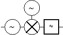
Figure 33 Up- (or down-) converted electronically controlled oscillator.
A phase locked loop, see figure 34 is a third way. A high frequency voltage controlled oscillator (Kc) is frequency divided, phase compared (Kd) with a high quality lower frequency voltage controlled oscillator and the error signal is then fed into the control port of the high frequency voltage controlled oscillator. Kd is in unit V/rad and Kc in unit Hz/V. An interesting feature of the phase locked loop is the possibility to control the output frequency by controlling the division number in the frequency divider.
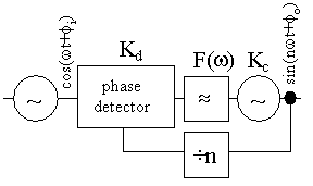
Figure 34 Phase locked loop frequency multiplied electronically controlled oscillator.
The phase noise levels in the phase locked loop in figure 34 can be analysed by simply redrawing it with phases instead of voltages, see figure 35. The "s" in the denominator for the transfer function of the voltage controlled oscillator is for phase, not frequency at the output, and the 2π in the numerator is for getting rad/s instead of Hz.
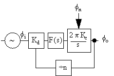
Figure 35 Phase locked loop frequency multiplied electronically controlled oscillator.
At the output we have (neglecting additional phase noise from the frequency divider and phase detector)
| (105) |
which solved for output phase equals
| (106) |
For example, suppose we implement the filter F(s) for proportional integrating (= PI) control characteristics, then
| (107) |
inserting it into (106) we get
| (108) |
| (109) | |||||||||||||||||||||||||||||||||||||||||||||||||||||||||||||||||||||||||||||||||||
| (110) |
where
| (111) |
The single sideband noise to carrier ratio becomes (2), (5), (110)
| (112) | ||||||||||||||||||||||||||||||||||||||||||||||||||||||||||||||||||||||||||||||||||||||||||||||||
First consider (112) inside the loop bandwidth ωn, that is s/ωn<<1, then we get using (2) and (5)
| (113) |
The same result as for a normal multiplier (104). The output phase noise equals the multiplied phase noise of the lower frequency oscillator. Finally consider (112) outside the loop bandwidth ωn, that is s/ωn>>1 which gives using (2) and (5)
| (114) |
Which is the same phase noise as the higher frequency voltage controlled oscillator.
Of course, combinations of the above, for example as in figure 36 are possible.
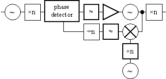
Figure 36 Complex oscillator structure.
Noise from the phase detector in a phase locked loop can be reduced with a different phase locked loop [52], see figure 37. An exclusive-or gate is used, to increase the phase detector sensitivity, together with a phase detector for to overcome the narrow pull in range of the exclusive-or gate.
Figure 37 Alternatively phase locked loop frequency multiplied electronically controlled oscillator.
A simple frequency discriminator consists of a delay line and a phase detector, see figure 38. It basically transforms frequency into voltage, the inverse of a voltage controlled oscillator.
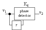
Figure 38 Frequency discriminator.
The operation is as follows. Fine tune the time delay into
| (115) |
where n is an integer. At the input ports of the phase detector we then have
| cos(ωt) | (116) |
and
| cos[ω(t−τ)] = cos(ωt−ωτ) = cos(ωt−2πfτ) = cos[ωt−2π(fr+f0)τ] = = cos(ωt−2πfrτ−2πf0τ) = cos(ωt−2πfrτ−2πn) = cos(ωt−2πfrτ) |
(117) |
After phase comparing we have at the output
| v2 = 2πfrτKd | (118) |
which is a baseband voltage proportional to the frequency deviation fr. Another possible implementation is depicted in figure 39.
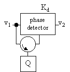
Figure 39 Frequency discriminator.
In this case we have at the phase detector output port, using (62)
| (119) |
where the first approximation is a expansion into a Taylor series. This is also a baseband voltage proportional to the frequency deviation fr. Comparing the proportionality constants of (118) and (119) one finds that it's simply equation (67), the delay line quality factor relationship.
A basic frequency discriminator stabilised voltage controlled oscillator is depicted in figure 40. The voltage controlled oscillator's frequency output is transformed into a error voltage by the frequency discriminator. The error voltage is then fed back to the control port, as in an usual control loop.
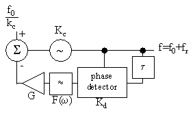
Figure 40 Frequency discriminator stabilised oscillator.
The same configuration can be redrawn with phases instead, see figure 41.
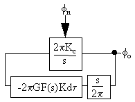
Figure 41 Frequency discriminator stabilised oscillator.
We have at the output
| (120) |
With sufficient time delay τ, gain G and stability considerations the phase noise can be decreased. The spectral density of phase fluctuations becomes
| (121) |
where SΦ0 is the unstabilised spectral density of phase fluctuations. Notation with quality factor instead of time delay using equation (67) and assuming 2πτKdF(s)GKc>>1 gives
| (122) |
where QLE is the loaded quality factor of the outer resonator (the resonator in the frequency discriminator). The equation has similarities to Leeson's equation (65). Inserting (65) one gets
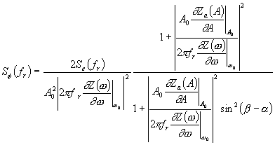
| (123) |
where QLI is the loaded quality factor of the internal resonator (the resonator in the voltage controlled oscillator). As the loop gain increases other noise sources than those in the voltage controlled oscillator will start dominating [10], [19], [53]. A problem with this type of frequency discriminator stabilised voltage controlled oscillators is to tune the two resonators to exactly the same resonant frequency so that phase errors do not contributes to the phase noise [12]. One solution to this problem is depicted in figure 42, [16], [23], [54], [55]. In this configuration, a common resonator, labelled "Q" is used in both the oscillator loop and in the frequency discriminator loop. The electronically controlled phase shifter labelled "Φ" tunes the frequency of oscillation.
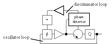
Figure 42 Single resonator frequency discriminator oscillator.
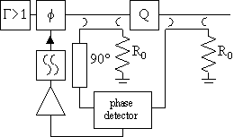
Another solution to the problem is depicted in figure 43, [56], [57], where the scattering parameters in the smith chart refer to the resonator labelled "Q", and the arrows indicate increasing frequency.
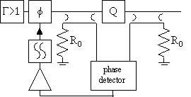
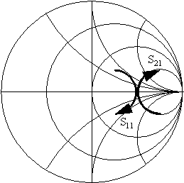
Figure 43 Single resonator frequency discriminator oscillator.
The operation is as follows: The couplers provides signals proportional to the scattering parameters S11 and S21 of the resonator. They are in phase at resonance but quickly changes as the frequency changes from resonance as can be seen in figure 43. The phase difference between the two deflected signals is thereby by first order approximation proportional to the difference between the operating frequency and the resonance frequency. The phase difference is detected by a phase detector, amplified, filtered and fed back to an electronically controlled phase shifter that control the operating frequency. A control loop that keeps the operating frequency equal to the resonant frequency has thereby been established. The control loop also compensates for slow variations in the operating frequency caused by low frequency noise, and thereby lowers the phase noise.
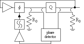
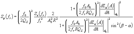
A third implementation is depicted in figure 44, [58], see Appendix C. Here, some of the incident wave onto the resonator and some of the transmitted wave passing through the resonator are deflected by couplers and phase compared. The resulting signal representing a phase error in the oscillation loop is then negatively fed back into the oscillation loop. A 90° phase shift transmission line is needed to compensate for the additional phase shift of the transmitted wave passing through the resonator and both couplers. Phase noise improvement of 10 dB have been demonstrated, see Appendix C. The phase noise improvement is expected to be limited by the low frequency noise level in the discriminator feedback loop.
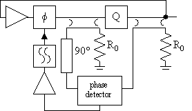
Figure 44 Single resonator frequency discriminator oscillator.
The two ideas described in figure 43 and figure 44 can be extended into a set of topologies as presented here in this table for the first time:
| Transmission mode oscillator | Reflection mode oscillator | |
 |  | |
 | |  |
 |  |  |
Two active devices in a balanced configuration can reduce oscillator phase noise [8], [40], [59], [60]. The balanced operation is supposed to prevent direct mixing of the low frequency noise with the carrier in the same way as a balanced mixer prevents unwanted mixing products. Another possible explanation to the effect is that a decreased bias current level in the device decreases the low frequency noise. The decreased bias current level is accomplished by operating the amplifying part in a non-class-A operation, such as class-B or class-C. Practical noise reduction have been about 10 dB. The technique of balanced operation is also used for the frequency controlling device, see figure 31.
The transposed gain amplifier [61], see figure 45, first down-converts the carrier frequency, amplifies at the down converted frequency and finally up-convert to the original carrier frequency. This enables the use of a relatively low frequency silicon bipolar transistor amplifier with little low frequency noise to be used instead of the traditional high frequency field effect transistor amplifier with more low frequency noise. The oscillator in the transposed gain amplifier does not need to be a high quality oscillator.
Figure 45 Transposed gain amplifier.
High spectral purity microwave signals can be produced by mixing two laser sources with different wavelengths [62].
The possibility to decrease the phase noise by the calculation of the optimum values for a set of variables for a given circuit topology is of course a highly wanted feature to the circuit designer. It is equally obvious, if such a procedure is to be successful, that one needs accurate models and a method for the optimisation. Methods are known [63], [64], [65].
A model that can predict phase noise should contain the low-frequency noise. Since the device is operating in a non-linear mode, it is not possible to simply extract the internal noise sources to two outer noise sources and a correlation impedance as is the case with linear circuits (e.g. amplifiers) [5], [66]. The non-linear operation can (and will) alter the bias point, and thereby alter the noise source levels [43]. It is often possible to get calculated and measured data to coincide, but when optimising with simple models one will most probably get non-physical results such as zero phase noise. A reason for this is that the oscillator pushing factor can be zero at some bias points [66], [43]. The optimiser will of course present that erroneous lowest number. Also, authors have found low correlation between the low frequency drain noise and the oscillator phase noise [43], [44], [45].
The most simple way to model the effect of low frequency noise is by inserting one noise generator at the gate (or base) of a noiseless non-linear model, see figure 46. [67], [68], [39], [40].
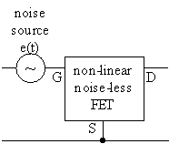
Figure 46 Non-linear model with low-frequency noise.
A somewhat improved model is a noise voltage source at the gate and a noise current source at the drain, see figure 47. [69], [70]
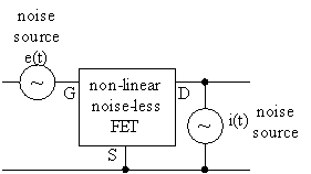
Figure 47 Non-linear model with low-frequency noise.
A model for correlating phase noise and low frequency noise has been presented [45], see figure 48.
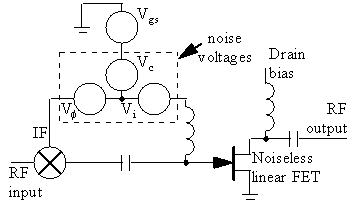
Figure 48 Linear model with low-frequency noise effects.
In [66] and [71] a model with two noise sources distributed along the channel is proposed, see figure 49.
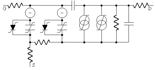
Figure 49 non-linear model with low-frequency noise.
Some of the reported methods are costly, complex or difficult to design.
For a simple low phase noise design it's often sufficient with a moderate quality factor resonator, such as a cavity resonator or a dielectric resonator. It is highly important that the frequency of oscillation is equal to the resonators resonant frequency, so that the oscillator operates at the resonators steepest phase-to-frequency-derivative. The choice of device, preferably a silicon bipolar transistor and consideration of its related bias point and bias impedances should be done carefully as well.
The multiplication of a low frequency source using a phase locked loop or cascaded frequency multipliers are the most usual methods for slightly higher performance.
Other methods are not so common, but sometimes find their use in extraordinary cases.
I express my thanks to professor Iltcho Angelov, professor Erik Kollberg and professor Herbert Zirath for their valuable comments on this work.
This work was supported by Chalmers Centre for High Speed Technology.
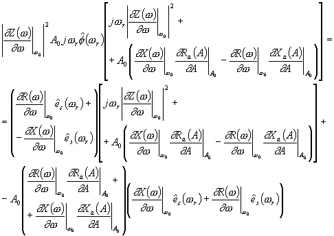
inserting (87) and (88) in (89) one gets
| (124) | ||||||||||||||||||||||||||||||||||||||||||||||||||||||||||||||||||||
and using (83) it simplifies to
| (125) | |||||||||||||||||||||||||||||||||||||||||||||||||||||||||||||||
which can be rearranged into
| (126) | |||||||||||||||||||||||||||||||||||||||||||||||||||||||||||||||||||||||||||||||||||||||
and further into
| (127) | |||||||||||||||||||||||||||||||||||||||||||||||||||||||||||||||||||||||||||||||||||||||||||||||||||||||||||||||||||
and finally into
| (128) | |||||||||||||||||||||||||||||||||||||||||||||||||||||||||||||||||||||||||||||||||||||||||||||||||||||||||||||||||
where the amplitude A(t) and phase Φ(t) are slowly time dependent. Now, let
| (129) | ||||||||||||||||
and insert (128) keeping in mind that the amplitude A(t) and phase Φ(t) only varies slowly one get
| (130) | ||||||||||||||||||||||||||||||||||||||||||||||||||||||||||||||||||||||||||||||||||||||||||||||||||||||||||||||||||||||||||||||||
utilising the substitution
| (131) |
gives
| (132) | ||||||||||||||||||||||||||||||||||||||||||||||||||||||||||||||||||||||||||||||||||||||||||||||||||||||||||||||||||||||||||||
which equals
| (133) | ||||||||||||||||||||||||||||||||||||||||||||||||||||||||||||||||||||||||||||||||||||||||||||||||||||||||||||||
and finally results in
| (134) |
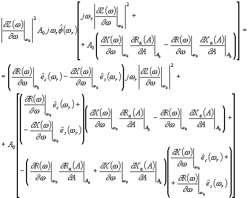
similarly letting
| (135) | ||||||||||||||||
results in
| (136) |
| setting (134) | 1 | ∂X(ω) | ω0 | +(136) | 1 | ∂R(ω) | ω0 | and | (134) | 1 | ∂R(ω) | ω0 | −(136) | 1 | ∂X(ω) | ω0 | one gets | ||||
| A(t) | ∂ω | A(t) | ∂ω | A(t) | ∂ω | A(t) | ∂ω |
| (137) | ||||||||||||||||||||||||||||||||||||||||||||||||||||||||||||||||||||||||||||||||||||||||||||||||||||||||||||||||||||||||||||||||||||||||||||||||||||||||||||||||
multiplying by the amplitude A(t), introducing the amplitude distortion δA(t)=A(t)−A0, realising that the time derivative of the amplitude A(t) is equal to the time derivative of the amplitude distortion δA(t) and neglecting the small terms δA²(t) and
| δA(t) | ∂Φ(t) | one find |
| ∂t |
| (138) |
The nearest homogenous equivalent to the first differential equation is
| (139) |
which can be solved trough separation
| (140) |
giving
| (141) |
and finally
| (142) |
which will only converge if
| (143) |
Taking the Fourier transform on equation (138) one gets
 | (144) |
rearranging the first equation and inserting it into the second gives
 | (145) |
⇒
 | (146) |
⇒
 | (147) |
⇒
 | (148) |
⇒
 | (149) |
⇒
 | (150) |
⇒
 | (151) |
Taking the square of the absolute value, and dividing by 2 one gets the spectral density of phase fluctuations
 | (152) |
Now, since ec(t) (129) and es(t) (135) represent the cosine and sine components of the distortion voltage e(t) in figure 27 we have [27]
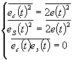 | (153) |
 | (154) |
A similar deduction can be found in [27]. Now, inserting (91) and (92) into (154) one gets
 | (155) |
which equals
 | (156) |
Going back to the resonator in figure 15, the impedance from (53) is
| (157) |
with the derivative at resonance being
 | (158) |
Utilising (55) it becomes
 | (159) |
The parallel case gives exactly the same expression. Inserting (159) into (156) one gets
 | (160) |
which equals
 | (161) |
If a resonator in an oscillator operates slightly off resonance the phase noise performance will very quickly be degenerated [12]. The situation appears if the resonator's resonant frequency isn't identical with the frequency of oscillation. The discrepancy is sometimes referred to as a phase error and can arise from manufacturing tolerances.
Also, the always present low frequency noise modulates voltage dependent reactances and thereby alters the frequency of oscillation [11], [2].
The use of a frequency discriminator is a well known technique for reducing these phase errors, and thereby improving the phase noise performance of oscillators. Some established frequency discriminator topologies suffers from the difficulty of synchronising two resonators (or a delay line and a resonator), while more recent topologies exhibit structures with a common resonator were the synchronisation problem has been eliminated.
A former topology for a frequency discriminator stabilised transmission mode oscillator with common resonator includes a circulator [54], [23], [55], [16], see figure 42. Another former topology for a frequency discriminator stabilised oscillator with common resonator is based on the reflection mode oscillator [56], [57], see figure 43.
This work presents a frequency discriminator stabilised transmission mode oscillator with common resonator that doesn't include any circulator.
The topology for the frequency discriminator stabilised transmission mode oscillator with common resonator is depicted in figure 50. The oscillator part is depicted at the top of the figure. It includes an electronically controlled phase shifter Φ for frequency tuning, a power generating amplifier and a resonator Q.
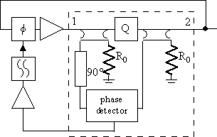
Figure 50 Frequency discriminator stabilised transmission mode oscillator with common resonator. The part surrounded by the broken line square is initially simulated separately.
On both sides of the resonator there are 90° directional couplers that couples some of the incident and transmitted wave through the resonator to a phase detector. A 90° phase shift transmission line is included for compensating the longer path of the transmitted wave, passing trough the resonator and both 90° couplers. The two waves incident onto the phase detector are therefore in phase at the resonator's resonant frequency f0, since the phase shift through the resonator is zero at resonance. For frequencies slightly off resonance there will be a phase difference between the two waves proportional to the product of the frequency deviation from resonance and the loaded quality factor of the resonator, see equation (64). The phase difference is monitored by a phase detector and fed back to the frequency tuning phase shifter in the oscillator loop. The signal from the phase detector is amplified and filtered, possibly with PI (= proportional and integrating) characteristics. In this way the frequency fluctuations are decreased and the phase noise lowered.
The frequency discriminator part, including the resonator, surrounded by the broken line square in figure 50, was simulated using HP-EEsof MDS microwave engineering software. Simulation input data for this general case is presented in figure 51. The simulation results in figure 52 shows the frequency discriminator output voltage and the phase shift of the resonator versus the frequency. figure 53 shows scattering parameters for the resonator.
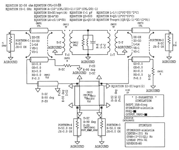
Figure 51 Circuit diagram used as simulation input data.
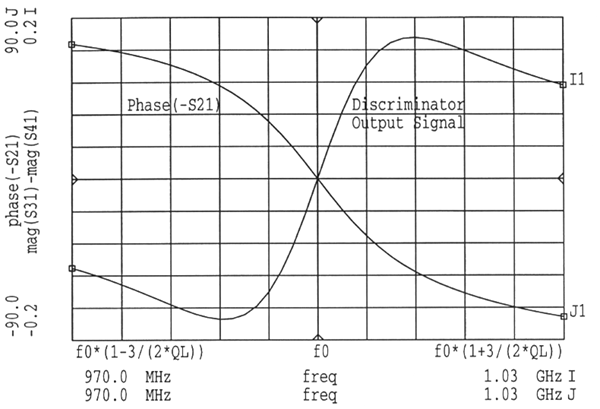
Figure 52 Phase shift and output voltage for the frequency discriminator part, including the resonator.
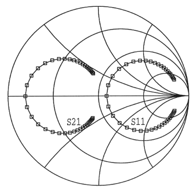
Figure 53 Scattering parameters for the frequency discriminator part, including the resonator. Center frequency f0 is 1 GHz and the bandwidth is 3*f0/QL = 60 MHz.
Using this topology, a circuit was designed in microstrip technology on a 15 mil RT Duroid 5870 substrate, see figure 54.
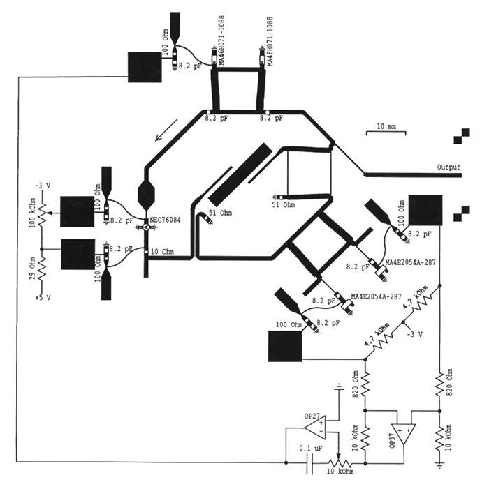
Figure 54 Circuit for a 4,6 GHz oscillator.
For the microwave amplifier, to the left in figure 54, a NEC 76084 GaAs MESFET transistor was used. The phase shifter, at the top of figure 54, consisted of a 3 dB branch line coupler and two MA46H071-1088 GaAs hyperabrupt varactors.
The phase detector, at the lower right hand corner of the layout part in figure 54, consisted of a 3 dB branch line coupler and two amplitude detectors. The detectors consisted of biased MA4E2054A-287 silicon schottky diodes. The detectors were connected to the 3 dB branch line couplers port number 2 and 3 with port numbering as depicted in figure 55.
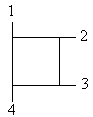
Figure 55 Branch line coupler port numbering.
With waves incident at port 1 and 4 forming an incident wave vector
| (162) |
and the 3 dB branch line coupler's scattering matrix being [15]
| (163) | ||||||||||||||||||||||||||||
the reflected wave vector becomes
| (164) | ||||||||||||||||
After the detectors and the differential base band amplifier we have
| (165) | |||||||||||||||||||||||||||||||||||||||||||||||||||||||||||||||||||
| (166) |
Which is indeed a phase detector output signal.
The resonator's loss, at the centre of figure 54, causes the power level at the output port to be lower (~ −6 dB) than the power level at the input port. To get approximately the same power level at the two ports entering the phase detector, the coupler at the resonator's input port has less (~ −6 dB) coupling compared to the coupler at the output port. Due to manufacturing tolerances at the etching process it was decided to implement the output port coupler as a branch line coupler, and the input port coupler as a coupled lines coupler to achieve the ~ 6 dB difference in coupling.
The control loop utilising PI control characteristics had low noise operational amplifiers OP37 and OP27. The OP37 was used as a differential amplifier and the OP27 was used as a PI-amplifier with adjustable gain.
The circuit and some identical separate subparts of it were etched and assembled. Measurements of the microwave amplifier part is presented in figure 56. It is well matched and provides 10 dB gain over a reasonable bandwidth.
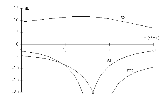
Figure 56 Measured microwave amplifier performance.
The frequency discriminator part, including the resonator was also manufactured as a separate block. Measurement results showing its transmission phase slope and detector output voltage is presented in figure 57. Some unimportant unbalance resulting in a small non-zero frequency discriminator output voltage at the steepest phase to frequency derivative can be observed. The measurement results shown in figure 57 are quite similar to the simulation results in figure 52.
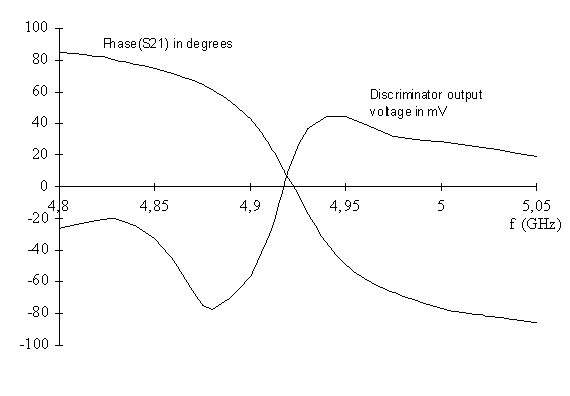
Figure 57 Resonator—frequency discriminator measurements.
The frequency discriminator signal is then amplified with PI control characteristics and fed back into the oscillation loop via the phase shifter. The phase shifter was manufactured and measured separately too. The measurement results are presented in figure 58.
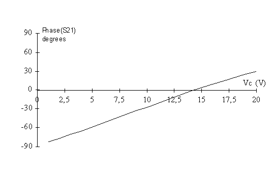
Figure 58 Phase shifter measurement.
The resonator in the complete oscillator circuit needed some tuning for the oscillation to start. The resonant frequency was slightly lowered to about 4,6 GHz from originally intended 5 GHz. The reason for this was insufficient modelling of the microstrip resonator and of the microwave transistor. After the tuning, the oscillator circuit performance was measured. The phase noise was measured using the discriminator method with and without closing the phase noise reduction control loop. figure 59 shows the phase noise with the control loop broken, and figure 60 shows the phase noise with the control loop activated. A 10 dB improvement is observed.
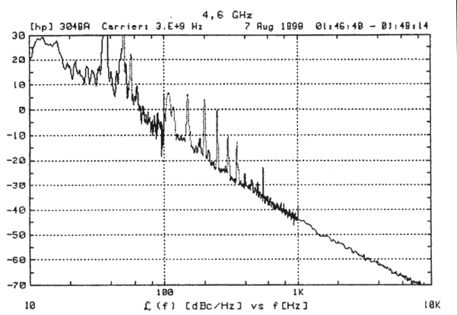
Figure 59 Phase noise with control loop broken.
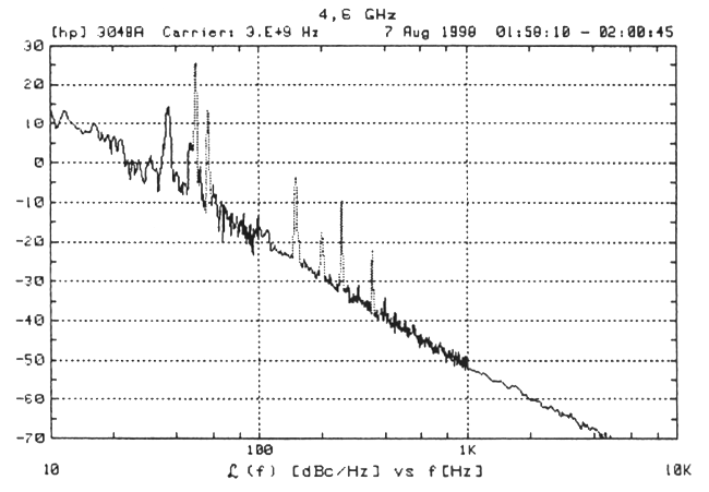
Figure 60 Phase noise with control loop closed.
The resulting phase noise level is remarkable low. It is measured to be approximately −52 dBc/Hz at 1 kHz off carrier. Multiplying the oscillator output into a 15 GHz oscillator using equation (104) and calculating the phase noise at 100 kHz off carrier assuming a 30 dB slope per decade equals
| (167) |
A carefully designed MESFET microstrip oscillator at 15 GHz is reported to have a phase noise level of approximately −100 dBc/Hz at 100 kHz off carrier [65], an exceptionally low value for this type of oscillator.


